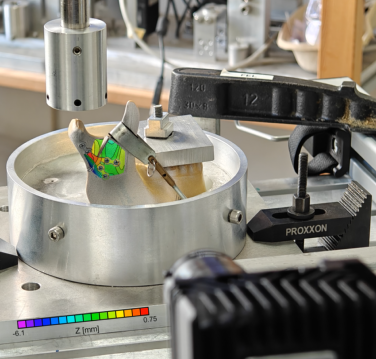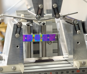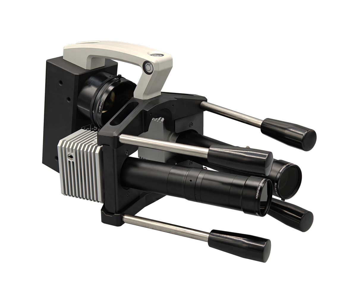
Combination of a special stereomicroscope with Vic-3D digital image correlation on electronic components.
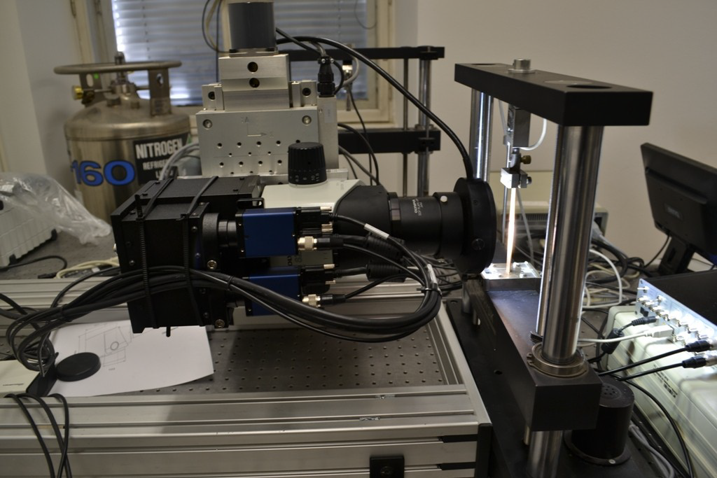
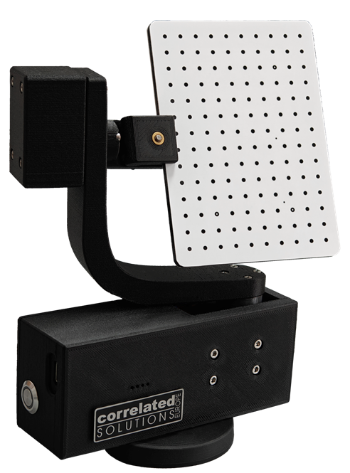
Measurement set up: Stereo microscope mounted
on x‑y-z-microtable (backside) and tensile machine (right).
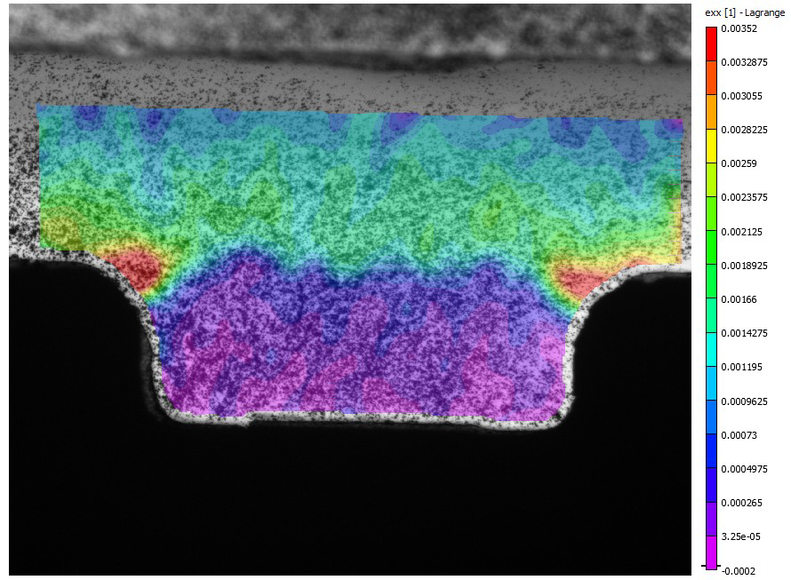
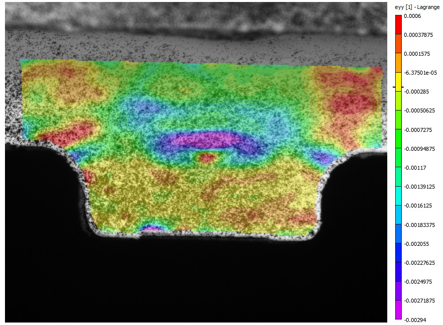
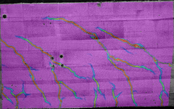
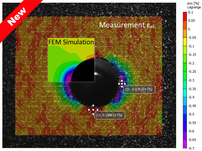
Servered ceramic capacitor chip under bending load (image width approx. 4mm):
Strain in x‑direction (upper image) and y- direction (lower image).
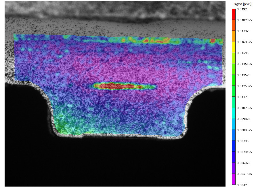
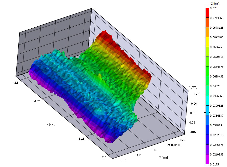
Standard derivation (upper) under load : An increased value occurs on the middle against the reference
state by the locally small bulge at the contact between chip and board (see 3D conture below). This might be caused
by material , which is pressed together between the two parts (including the colour layer). In the upper area the
increased values of the standard derivation is caused by the reduced speckle density.